6 inch silicon wafers play a crucial role in the electronics industry, serving as the backbone for semiconductor manufacturing. These wafers form the basis for a wide array of electronic devices and systems. The market for 6 inch silicon wafers is experiencing significant growth, with a projected compound annual growth rate (CAGR) of 7.10% from 2024 to 2031. This growth highlights their increasing importance in technological advancements and innovation. As foundational components, these wafers enable the production of microchips and integrated circuits, which are essential for modern electronics.
Key Takeaways
- 6 inch silicon wafers are essential for semiconductor manufacturing, serving as the foundation for microchips and integrated circuits that power modern electronics.
- Their standardized size allows for efficient fabrication processes, making them a preferred choice in the industry and contributing to a projected market growth of 7.10% from 2024 to 2031.
- These wafers play a critical role in high-speed communication by acting as substrates for chips that facilitate rapid data transfer, essential for internet connectivity.
- In sensor technology, 6 inch silicon wafers are used to develop environmental and automotive sensors, enhancing safety and efficiency in various applications.
- The wafers are also vital in renewable energy systems, providing substrates for semiconductors in solar and wind power inverters, thus supporting sustainable energy solutions.
- Their cost-effectiveness and production efficiency stem from economies of scale, allowing manufacturers to reduce costs and minimize waste during production.
- 6 inch silicon wafers are invaluable in research and development, providing a reliable platform for experiments and advancements in semiconductor technology.
Applications of 6 Inch Silicon Wafers

Semiconductor Manufacturing
6 inch silicon wafers serve as the foundation for semiconductor manufacturing. They are integral to the production of microchips and integrated circuits, which power countless electronic devices. These wafers provide a stable and reliable substrate for the intricate processes involved in creating these components. The standard size of 6 inches (150 mm) allows for efficient fabrication, making them a preferred choice in the industry.
Microchip and Integrated Circuit Production
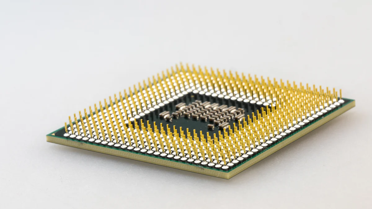
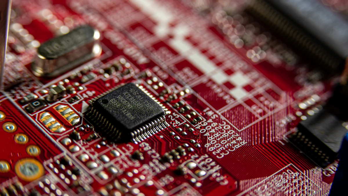
Microchips and integrated circuits form the core of modern electronics. Manufacturers use 6 inch silicon wafers to produce these essential components. The wafers’ uniformity and high-quality surface ensure precise etching and layering, which are crucial for the functionality of microchips. This precision enables the creation of complex circuits that drive everything from smartphones to computers.
High-Speed Communication Chips
In the realm of high-speed communication, 6 inch silicon wafers play a pivotal role. They act as substrates for chips used in Wide Area Network (WAN) communications. These chips facilitate rapid data transfer, supporting the backbone of internet connectivity and telecommunications. The wafers’ ability to support high-frequency operations makes them indispensable in this sector.
Sensor Technology
The versatility of 6 inch silicon wafers extends to sensor technology. They are used in the development of various sensors that monitor environmental conditions and enhance automotive systems. The wafers’ properties allow for the integration of sensitive detection elements, ensuring accurate and reliable sensor performance.
Environmental and Automotive Sensors
Environmental sensors, which track parameters like temperature and humidity, rely on 6 inch silicon wafers for their construction. In the automotive industry, these wafers contribute to the development of sensors that improve vehicle safety and efficiency. Their role in sensor technology underscores their importance in advancing smart and sustainable solutions.
Renewable Energy Systems
6 inch silicon wafers also find applications in renewable energy systems. They are crucial in the production of components for solar and wind power inverters. These inverters convert energy from renewable sources into usable electricity, playing a key role in the transition to sustainable energy solutions.
Solar and Wind Power Inverters
In solar and wind energy systems, inverters are essential for converting direct current (DC) into alternating current (AC). 6 inch silicon wafers provide the necessary substrate for the semiconductors used in these inverters. Their efficiency and reliability ensure optimal performance, contributing to the effectiveness of renewable energy technologies.
Research and Development
In the realm of research and development, 6 inch silicon wafers serve as indispensable tools. Researchers utilize these wafers to explore new materials and technologies, pushing the boundaries of what is possible in electronics. Their standard size and high-quality surface make them ideal for experimental setups and testing environments.
Substrate Studies and Microscopy
6 inch silicon wafers play a pivotal role in substrate studies and microscopy. Scientists often use these wafers as substrates for various analytical techniques, including Atomic Force Microscopy (AFM) and Scanning Electron Microscopy (SEM). These techniques require a stable and uniform surface to produce accurate and reliable results. The wafers’ consistent quality ensures that researchers can focus on their experiments without worrying about substrate variability.
-
Substrate Studies: Researchers conduct substrate studies to understand the interaction between different materials and the silicon wafer. This knowledge is crucial for developing new semiconductor devices and improving existing technologies.
-
Microscopy Applications: In microscopy, the wafers provide a flat and smooth surface necessary for high-resolution imaging. This allows scientists to observe and analyze the microstructures of materials with precision.
The use of 6 inch silicon wafers in research and development highlights their versatility and importance in advancing scientific knowledge. By providing a reliable platform for experimentation, these wafers contribute significantly to technological innovation and discovery.
Advantages of 6 Inch Silicon Wafers

Cost-Effectiveness
6 inch silicon wafers offer significant cost advantages in the electronics industry. Their widespread use in semiconductor manufacturing allows companies to benefit from economies of scale. As production volumes increase, the cost per wafer decreases, making them an economical choice for large-scale operations.
Economies of Scale
Manufacturers achieve economies of scale by producing 6 inch silicon wafers in bulk. This large-scale production reduces the overall cost of manufacturing, as fixed costs are spread over a greater number of units. Companies can then pass these savings on to consumers, making electronic devices more affordable.
Material Efficiency
Material efficiency is another key advantage of 6 inch silicon wafers. The wafers’ size allows for optimal use of silicon material, minimizing waste during the production process. This efficient use of resources not only reduces costs but also supports sustainable manufacturing practices.
Production Efficiency
The production efficiency of 6 inch silicon wafers enhances their appeal in the electronics sector. Their standardized size and compatibility with existing equipment streamline manufacturing processes, leading to faster production times and reduced operational costs.
Streamlined Processes
6 inch silicon wafers facilitate streamlined manufacturing processes. Their uniform dimensions allow for consistent handling and processing, reducing the likelihood of errors and defects. This consistency improves overall production efficiency and ensures high-quality output.
Equipment Compatibility
Equipment compatibility is a crucial factor in the production of 6 inch silicon wafers. Most semiconductor fabrication facilities are equipped to handle this standard wafer size, allowing for seamless integration into existing production lines. This compatibility reduces the need for costly equipment upgrades and ensures smooth operations.
6 inch silicon wafers are indispensable in modern electronics, offering a multitude of applications and benefits. They serve as the backbone of semiconductor manufacturing, enabling the production of essential components like microchips and integrated circuits. Their efficiency and cost-effectiveness make them a preferred choice over larger wafers, which, although offering higher production efficiency, come with increased material costs. The versatility of 6 inch silicon wafers extends to sensor technology, renewable energy systems, and research, underscoring their critical role in technological advancement and innovation.
FAQ
What are 6-inch silicon wafers?
6-inch silicon wafers are thin slices of semiconductor material, specifically silicon, with a diameter of 150 mm. They serve as the foundational substrate for manufacturing various electronic components, including integrated circuits and microchips.
Why are 6-inch silicon wafers important in electronics?
6-inch silicon wafers are crucial in electronics due to their role in semiconductor manufacturing. They enable the production of integrated circuits, which power devices like smartphones, computers, and sensors. Their standard size facilitates efficient fabrication processes, making them a preferred choice in the industry.
How do 6-inch silicon wafers contribute to renewable energy?
In renewable energy systems, 6-inch silicon wafers are used in the production of solar panels and wind power inverters. They provide the necessary substrate for semiconductors that convert energy from renewable sources into usable electricity, supporting the transition to sustainable energy solutions.
What advantages do 6-inch silicon wafers offer in semiconductor manufacturing?
6-inch silicon wafers offer several advantages, including cost-effectiveness and production efficiency. Their standardized size allows for economies of scale, reducing manufacturing costs. Additionally, their compatibility with existing equipment streamlines production processes, enhancing overall efficiency.
How do 6-inch silicon wafers support research and development?
Researchers use 6-inch silicon wafers in various experimental setups, including substrate studies and microscopy. Their high-quality surface and standard size make them ideal for testing new materials and technologies, contributing to advancements in scientific knowledge and innovation.
Are 6-inch silicon wafers used in sensor technology?
Yes, 6-inch silicon wafers play a significant role in sensor technology. They are used in the development of environmental and automotive sensors, providing a stable substrate for integrating sensitive detection elements. This ensures accurate and reliable sensor performance.
What role do 6-inch silicon wafers play in high-speed communication?
In high-speed communication, 6-inch silicon wafers act as substrates for chips used in Wide Area Network (WAN) communications. These chips facilitate rapid data transfer, supporting internet connectivity and telecommunications infrastructure.
How have silicon wafer sizes evolved over time?
Silicon wafer sizes have evolved to meet the demand for smaller and more powerful electronic devices. The industry has transitioned from smaller wafers to larger ones, like the 6-inch size, to accommodate the increasing complexity and miniaturization of modern electronics.
What is the significance of 6-inch SiC wafers in electronics?
6-inch SiC (Silicon Carbide) wafers are essential for developing smaller, faster, and more energy-efficient electronics. They are particularly important in sectors like automotive, renewable energy, and industrial automation, where efficiency and performance are critical.
How do 6-inch silicon wafers support the miniaturization of electronics?
6-inch silicon wafers support the miniaturization of electronics by providing a precise and uniform substrate for creating intricate microchips and integrated circuits. This precision enables the development of compact and efficient devices, driving advancements in modern technology.