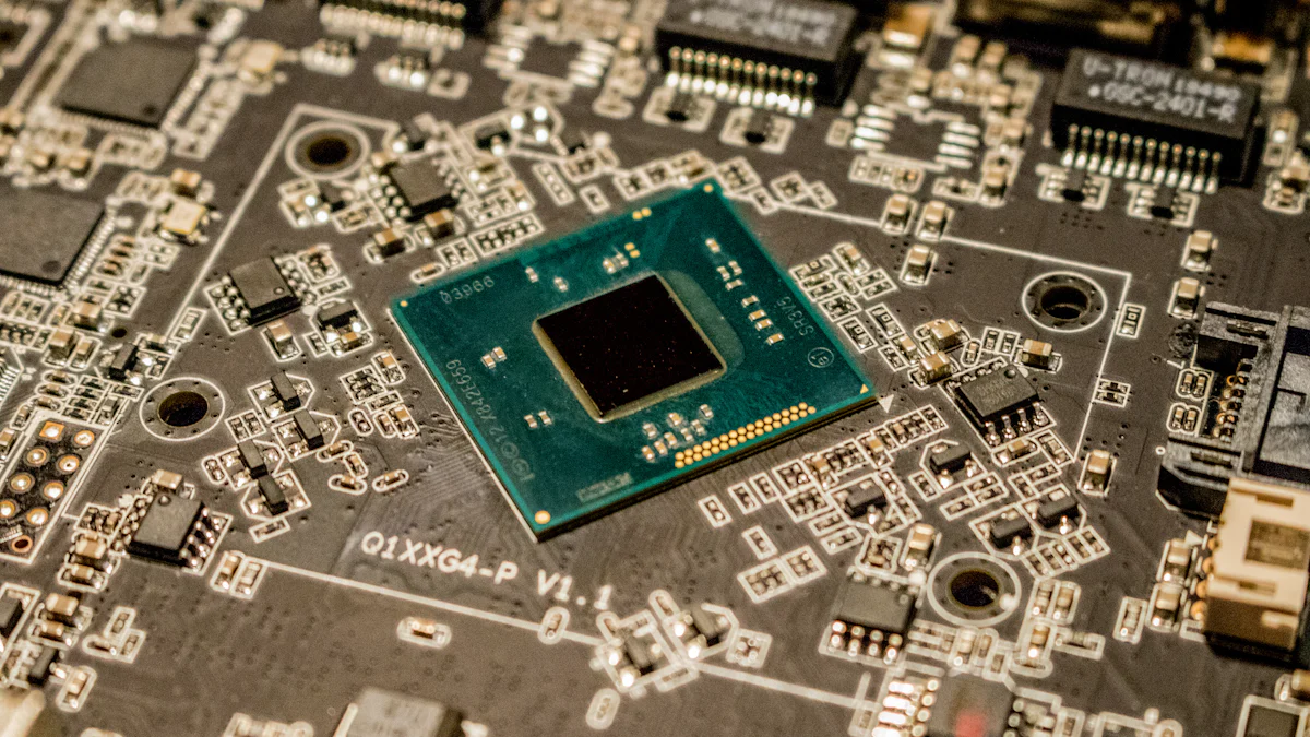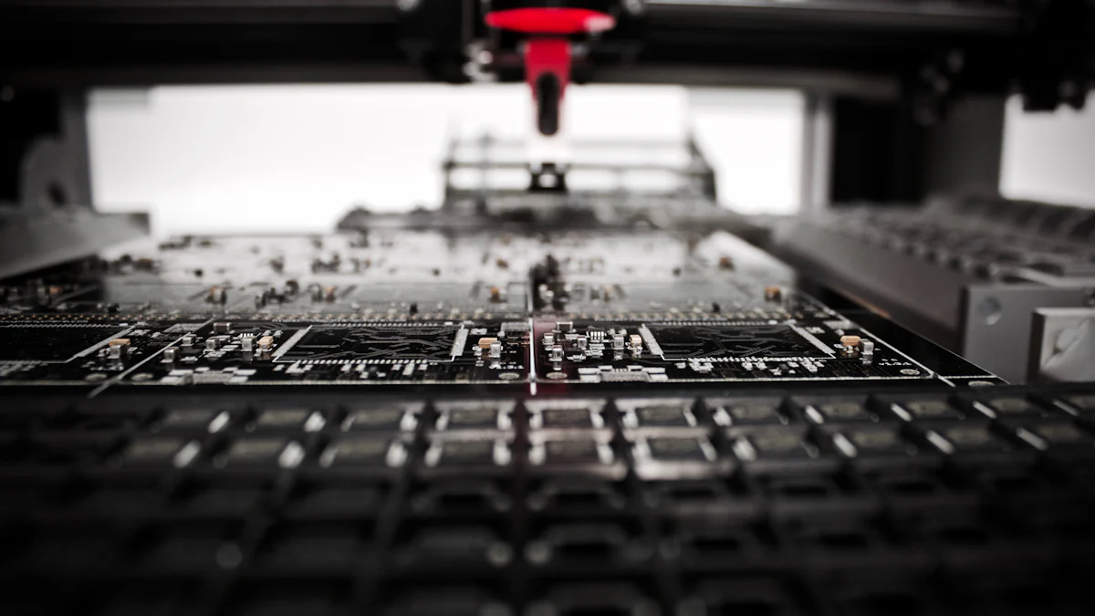
Applied Materials epitaxy plays a transformative role in modern electronics by enabling the precise growth of single-crystal layers on semiconductor substrates. This process enhances electron transmission, ensuring superior device performance. Advances such as remote epitaxy now allow manufacturers to create flexible, multifunctional chips while reusing expensive Applied Materials epitaxy trays, significantly reducing costs. Techniques like bandgap engineering and epitaxial regrowth are pushing transistors beyond current speed limits, driving innovations in high-power electronics and extreme-environment applications. By refining semiconductor structures, Applied Materials EPI technologies, including the cutting-edge Applied Materials EPI Prime, continue to shape the future of computing, communication, and energy-efficient devices.
Key Takeaways
- Applied Materials epitaxy is crucial for enhancing the performance of electronic devices by enabling the precise growth of single-crystal layers on semiconductor substrates.
- Ultra-Wide Bandgap (UWBG) materials, such as gallium oxide and aluminum gallium nitride, are revolutionizing power electronics by allowing devices to operate at higher voltages and temperatures.
- The integration of two-dimensional (2D) materials like graphene into epitaxial processes is paving the way for ultra-thin, flexible electronics with improved performance.
- Innovative techniques like Atomic Layer Epitaxy (ALE) and Selective Area Epitaxy (SAE) provide unparalleled control over material properties, essential for developing advanced transistors and multifunctional devices.
- Epitaxy is driving advancements in high-performance computing and AI by optimizing semiconductor structures for faster processing speeds and lower energy consumption.
- Sustainability in epitaxial processes is becoming a priority, with techniques that reduce waste and energy consumption while maintaining high-quality crystal growth.
- Emerging opportunities in quantum electronics highlight the importance of epitaxy in fabricating devices that manipulate quantum states, essential for the future of computing and communication.
Advances in Applied Materials Epitaxy for Electronics

Development of Ultra-Wide Bandgap (UWBG) Materials
Ultra-Wide Bandgap (UWBG) materials represent a significant leap forward in semiconductor technology. These materials, characterized by their ability to operate at higher voltages, frequencies, and temperatures, are transforming the landscape of power electronics. Researchers have made remarkable progress in understanding the physics of UWBG semiconductors, enabling the development of devices that outperform traditional silicon-based technologies.
For instance, UWBG materials like gallium oxide (Ga2O3) and aluminum gallium nitride (AlGaN) exhibit exceptional thermal stability and electrical conductivity. These properties make them ideal for high-power applications, such as electric vehicles and renewable energy systems. Recent studies have also highlighted their potential in extreme-environment electronics, where durability and efficiency are critical. By leveraging these advancements, applied materials epitaxy continues to refine the growth processes for UWBG materials, ensuring precise crystal quality and uniformity.
Integration of 2D Materials in Epitaxy
The integration of two-dimensional (2D) materials into epitaxial processes has opened new avenues for innovation in electronics. Materials like graphene, molybdenum disulfide (MoS2), and hexagonal boron nitride (h-BN) offer unique properties, including high electron mobility, mechanical flexibility, and atomic-scale thickness. These characteristics enable the creation of ultra-thin, lightweight devices with enhanced performance.
Applied materials epitaxy plays a pivotal role in achieving seamless integration of 2D materials with traditional semiconductors. Techniques such as van der Waals epitaxy allow for the growth of 2D layers without lattice mismatch issues, preserving their intrinsic properties. This advancement has paved the way for applications in flexible electronics, wearable devices, and next-generation transistors. The ability to combine 2D materials with conventional substrates also enhances the functionality of electronic components, driving innovation across multiple industries.
Innovations in Compound Semiconductors
Compound semiconductors, composed of two or more elements, are at the forefront of modern electronics. Materials like gallium arsenide (GaAs), indium phosphide (InP), and silicon carbide (SiC) offer superior performance compared to silicon in specific applications. These semiconductors excel in high-frequency, high-power, and optoelectronic devices, making them indispensable in fields such as telecommunications, aerospace, and photonics.
Recent innovations in applied materials epitaxy have significantly improved the growth techniques for compound semiconductors. Methods like molecular beam epitaxy (MBE) and metal-organic chemical vapor deposition (MOCVD) ensure precise control over layer thickness and composition. This precision enables the fabrication of advanced devices, such as high-electron-mobility transistors (HEMTs) and laser diodes, with unparalleled efficiency and reliability. As the demand for faster, more efficient electronics grows, the role of compound semiconductors and their epitaxial advancements becomes increasingly critical.
Cutting-Edge Techniques in Applied Materials Epitaxy
Atomic Layer Epitaxy (ALE)
Atomic Layer Epitaxy (ALE) has emerged as a groundbreaking technique in the field of applied materials epitaxy. This method enables the deposition of ultra-thin, atomically precise layers, ensuring unparalleled control over material thickness and composition. ALE operates by introducing precursor gases in a sequential manner, allowing each atomic layer to form one at a time. This precision makes ALE ideal for applications requiring nanoscale accuracy, such as advanced transistors and memory devices.
The ability of ALE to create defect-free layers has revolutionized semiconductor manufacturing. It supports the development of high-performance devices by enhancing electron mobility and reducing energy losses. Industries leveraging ALE benefit from its compatibility with a wide range of materials, including silicon, gallium nitride (GaN), and aluminum oxide. This versatility ensures that ALE remains a cornerstone of modern epitaxial processes, driving innovation in electronics.
Selective Area Epitaxy (SAE)
Selective Area Epitaxy (SAE) introduces a new level of customization in epitaxial growth. This technique allows material deposition only in predefined regions of a substrate, enabling the creation of intricate patterns and structures. SAE achieves this by using masks or templates to block unwanted areas, ensuring material growth occurs precisely where needed.
The advantages of SAE extend beyond patterning. It facilitates the integration of multiple materials on a single chip, paving the way for heterogeneous device architectures. For example, SAE enables the combination of silicon with compound semiconductors like indium phosphide (InP) or gallium arsenide (GaAs), enhancing device functionality. This capability is particularly valuable in photonics and optoelectronics, where precise material placement is critical. SAE continues to expand the possibilities of applied materials epitaxy by enabling complex designs and multifunctional devices.
Enhancements in Molecular Beam Epitaxy (MBE)
Molecular Beam Epitaxy (MBE) remains a cornerstone of epitaxial growth, particularly for compound semiconductors. This technique involves directing molecular or atomic beams onto a heated substrate under ultra-high vacuum conditions. MBE offers exceptional control over layer thickness and composition, making it indispensable for research and development in advanced electronics.
Recent advancements in MBE have further enhanced its capabilities. Innovations in beam flux control and substrate heating have improved material uniformity and reduced defects. These enhancements support the fabrication of high-performance devices, such as quantum wells and superlattices, which require precise atomic arrangements. MBE also excels in producing materials for high-frequency and high-power applications, including microwave transistors and laser diodes. By refining this technique, applied materials epitaxy continues to push the boundaries of what is achievable in semiconductor technology.
Applications of Applied Materials Epitaxy in Advanced Electronics

High-Performance Computing and AI
Applied materials epitaxy has become a cornerstone in advancing high-performance computing and artificial intelligence (AI). By enabling the growth of high-quality crystal layers, epitaxy enhances electron transmission efficiency, which is critical for the development of faster and more reliable processors. This precision allows semiconductor manufacturers to push the boundaries of transistor performance, ensuring that chips can handle the immense computational demands of AI algorithms and data-intensive tasks.
Epitaxial techniques, such as bandgap engineering, play a pivotal role in optimizing semiconductor structures for AI applications. These methods allow for the fine-tuning of electronic properties, resulting in devices with higher processing speeds and lower energy consumption. For instance, epitaxy facilitates the integration of compound semiconductors like gallium arsenide (GaAs) and silicon carbide (SiC), which are essential for creating high-electron-mobility transistors (HEMTs) used in AI accelerators. As AI continues to evolve, applied materials epitaxy remains at the forefront of enabling the next generation of intelligent systems.
Next-Generation Communication Systems
The rapid evolution of communication technologies, including 5G and beyond, relies heavily on advancements in epitaxial processes. Applied materials epitaxy enables the fabrication of high-frequency and high-power devices that are essential for next-generation communication systems. By depositing ultra-thin, defect-free crystal layers, epitaxy ensures the production of components with superior signal integrity and minimal energy loss.
Selective Area Epitaxy (SAE) and Molecular Beam Epitaxy (MBE) have proven instrumental in developing devices like microwave transistors and laser diodes. These components are critical for high-speed data transmission and optical communication networks. Additionally, epitaxy supports the integration of multiple materials on a single chip, enabling the creation of multifunctional devices that enhance the performance of communication systems. As the demand for faster and more reliable connectivity grows, epitaxial innovations continue to drive progress in this field.
Energy-Efficient Electronics
Energy efficiency has become a top priority in modern electronics, and applied materials epitaxy plays a vital role in achieving this goal. By refining semiconductor structures, epitaxy reduces energy losses and improves the overall performance of electronic devices. Techniques like remote epitaxy allow for the creation of flexible, multifunctional chips that consume less power while maintaining high performance.
Ultra-Wide Bandgap (UWBG) materials, such as gallium oxide (Ga2O3) and aluminum gallium nitride (AlGaN), have emerged as game-changers in energy-efficient electronics. These materials, enabled by advanced epitaxial growth processes, operate at higher voltages and temperatures, making them ideal for applications like electric vehicles and renewable energy systems. Furthermore, epitaxy facilitates the incorporation of metallic particles and magnetic elements within semiconductors, paving the way for ultrafast electro-optical components that consume less energy. By leveraging these advancements, applied materials epitaxy continues to shape a more sustainable future for electronics.
Challenges and Future Directions in Applied Materials Epitaxy
Overcoming Material and Process Limitations
The field of applied materials epitaxy faces significant challenges in addressing material and process limitations. Researchers encounter difficulties in achieving defect-free crystal growth, especially when working with complex materials like ultra-wide bandgap (UWBG) semiconductors and compound semiconductors. These imperfections can hinder device performance and reliability, particularly in high-power and high-frequency applications.
To overcome these obstacles, scientists are exploring advanced growth techniques and refining existing methods. For example, innovations in molecular beam epitaxy (MBE) and atomic layer epitaxy (ALE) have improved control over atomic-scale deposition, reducing defects and enhancing material uniformity. Additionally, the development of in-situ monitoring tools allows real-time adjustments during the epitaxial process, ensuring optimal crystal quality. By addressing these limitations, applied materials epitaxy continues to push the boundaries of semiconductor technology.
Sustainability in Epitaxial Processes
Sustainability has become a critical focus in the semiconductor industry, including epitaxial processes. Traditional methods often consume significant energy and generate waste, raising concerns about their environmental impact. The industry is now prioritizing eco-friendly practices to align with global sustainability goals.
Efforts to enhance sustainability include the adoption of energy-efficient epitaxial systems and the recycling of expensive substrates. Techniques like remote epitaxy enable manufacturers to reuse substrates without compromising crystal quality, reducing material waste. Furthermore, researchers are investigating alternative precursors and gases that minimize harmful emissions during the growth process. These advancements not only lower the environmental footprint but also reduce operational costs, making sustainable epitaxial processes a win-win for both the industry and the planet.
Emerging Opportunities in Quantum Electronics
Quantum electronics represents a promising frontier for applied materials epitaxy. The precise control offered by epitaxial techniques is essential for fabricating quantum devices, which rely on atomic-scale structures to manipulate quantum states. Materials like silicon-germanium (SiGe) and indium arsenide (InAs) are gaining attention for their potential in quantum computing and communication systems.
Recent breakthroughs in epitaxial growth have enabled the creation of quantum wells, quantum dots, and superlattices with unprecedented precision. These structures form the foundation of quantum devices, such as qubits and single-photon emitters. Additionally, the integration of 2D materials into epitaxial processes opens new possibilities for hybrid quantum systems. As the demand for quantum technologies grows, applied materials epitaxy will play a pivotal role in shaping this transformative field.
Applied materials epitaxy continues to revolutionize the electronics industry by advancing materials, techniques, and applications. Innovations like ultra-wide bandgap materials and remote epitaxy enable the creation of high-performance devices, from energy-efficient systems to flexible electronics. Techniques such as atomic layer epitaxy and selective area epitaxy ensure precision and scalability, driving breakthroughs in AI, communication, and quantum technologies. The future of epitaxy lies in sustainable practices and the integration of novel materials, promising a transformative impact on electronics. As these advancements unfold, epitaxy remains a cornerstone of innovation and progress.
FAQ
What is the epitaxy (epi) process in semiconductor fabrication?
The epitaxy process in semiconductor fabrication involves depositing a fine layer of single crystal, typically ranging from 0.5 to 20 microns, onto a single crystal substrate. This process ensures that the new crystalline layer grows in a specific orientation, matching the underlying substrate. It plays a critical role in creating high-quality materials for advanced electronic devices.
Why is the epitaxy process important in semiconductor manufacturing?
Epitaxy enables the growth of a higher-purity crystal layer on a substrate of the same material. This precision allows manufacturers to enhance the performance and reliability of semiconductor devices. In certain applications, such as Heterojunction Bipolar Transistors (HBTs) or Metal-Oxide-Semiconductor Field-Effect Transistors (MOSFETs), epitaxy supports the growth of material layers that differ from the substrate, expanding design possibilities.
What does the term “epitaxy” mean?
Epitaxy refers to a specialized form of crystal growth or material deposition. In this process, new crystalline layers form with one or more well-defined orientations relative to the crystalline seed layer. The resulting crystalline film, known as the epitaxial layer, exhibits exceptional structural and electronic properties.
How does epitaxy improve semiconductor device performance?
Epitaxy enhances device performance by enabling precise control over material properties, such as thickness, composition, and crystal orientation. This control reduces defects, improves electron mobility, and ensures uniformity across the wafer. These benefits are essential for high-performance applications like AI processors, 5G communication systems, and energy-efficient electronics.
What types of materials are commonly used in epitaxy?
Epitaxy often involves materials like silicon, gallium arsenide (GaAs), silicon carbide (SiC), and aluminum gallium nitride (AlGaN). These materials are chosen for their unique properties, such as high thermal stability, electrical conductivity, and compatibility with advanced semiconductor devices.
What are the main techniques used in epitaxial growth?
Several techniques are employed in epitaxial growth, including Molecular Beam Epitaxy (MBE), Atomic Layer Epitaxy (ALE), and Metal-Organic Chemical Vapor Deposition (MOCVD). Each method offers distinct advantages, such as atomic-scale precision, defect reduction, and compatibility with various materials.
Can epitaxy support the development of flexible electronics?
Yes, epitaxy plays a pivotal role in the development of flexible electronics. Techniques like remote epitaxy enable the growth of high-quality crystal layers that can be transferred to flexible substrates. This innovation supports the creation of lightweight, bendable devices for applications like wearable technology and foldable displays.
How does epitaxy contribute to sustainability in semiconductor manufacturing?
Epitaxy contributes to sustainability by enabling efficient material usage and reducing waste. Processes like remote epitaxy allow manufacturers to reuse expensive substrates without compromising crystal quality. Additionally, advancements in energy-efficient epitaxial systems and eco-friendly precursors help minimize the environmental impact of semiconductor production.
What industries benefit most from epitaxial advancements?
Industries such as telecommunications, automotive, aerospace, and renewable energy benefit significantly from epitaxial advancements. Applications include high-frequency communication devices, power electronics for electric vehicles, and durable components for extreme environments. Epitaxy also supports emerging fields like quantum computing and AI.
What is the future of epitaxy in electronics?
The future of epitaxy lies in the integration of novel materials, such as 2D materials and ultra-wide bandgap semiconductors, along with sustainable practices. These advancements will enable the development of next-generation devices with higher performance, lower energy consumption, and greater versatility. Epitaxy will remain a cornerstone of innovation in the electronics industry.