Wafers related to chips form the backbone of semiconductor manufacturing. These thin slices of silicon serve as the foundation for creating intricate electronic components. Each wafer contains multiple dies, which are small sections etched with precise circuitry. These dies eventually transform into chips, the essential units powering modern devices like smartphones and computers. The connection between wafers related to chips, dies, and chips highlights the meticulous engineering behind semiconductor production. Silicon wafers, known for their quality and reliability, play a pivotal role in ensuring the performance and efficiency of electronic devices.
Key Takeaways
foundational elements in semiconductor manufacturing, serving as the substrate for creating multiple integrated circuits (ICs).
- Silicon is the preferred material for wafers due to its excellent electronic properties, cost-effectiveness, and thermal conductivity.
- The process of photolithography is crucial for etching intricate circuit patterns onto wafers, directly impacting the performance of the final chips.
- Precision in wafer dicing is essential to maintain the integrity of the delicate circuits, ensuring high-quality dies for chip production.
- Packaging transforms individual dies into functional chips, protecting them and enabling seamless integration into electronic devices.
Testing is vital to ensure that each chip meets performance standards, with advancements in technology improving the efficiency of this process.
- The semiconductor industry significantly influences global economies, driving innovation and creating high-paying jobs while shaping the technological landscape.
Wafers: The Foundation of Semiconductor Manufacturing

What Are Wafers?
Wafers are thin, circular slices of semiconductor material, typically silicon, that serve as the foundation for creating integrated circuits (ICs). These wafers undergo a series of intricate processes to transform into functional components of electronic devices. Manufacturers produce wafers using ultra-pure silicon, ensuring high quality and reliability. The process begins with the Czochralski method, where a single crystal of silicon is grown and then sliced into thin wafers. Each wafer acts as a substrate on which intricate electronic circuits are etched, enabling the creation of multiple dies on a single wafer.
The unique properties of silicon wafers make them indispensable in the semiconductor industry. Their ability to conduct electricity under specific conditions allows for precise control over electronic functions. Additionally, their thermal conductivity ensures efficient heat dissipation, preventing overheating in devices. These characteristics highlight the critical role of wafers in modern electronics.
Why Silicon Is the Preferred Material for Wafers
Silicon dominates the semiconductor industry due to its exceptional electronic properties and abundance. It can function as both an insulator and a conductor, depending on the addition of impurities, a process known as doping. This versatility makes silicon ideal for creating the intricate circuits required in integrated circuits.
Cost-effectiveness also contributes to silicon’s popularity. As one of the most abundant elements on Earth, silicon offers a reliable and economical option for large-scale production. While other materials like gallium arsenide and silicon carbide are used for specialized applications, they account for a much smaller share of the market compared to silicon.
Silicon’s thermal properties further enhance its suitability for semiconductor manufacturing. Its high thermal conductivity ensures that heat generated during device operation dissipates efficiently. This prevents damage to electronic components and extends the lifespan of devices. These advantages solidify silicon’s position as the preferred material for wafers.
The Role of Wafers in Integrated Circuit Production
Wafers play a pivotal role in the production of integrated circuits, which are essential for modern electronics. Each wafer serves as a platform for fabricating multiple ICs, enabling the compact design and enhanced functionality of devices like smartphones, computers, and medical equipment. The manufacturing process involves several stages, including photolithography, etching, and doping, to create the intricate patterns of circuits on the wafer’s surface.
Once the circuits are etched, the wafer undergoes dicing, where it is sliced into individual dies. These dies are then packaged into chips, which power various electronic devices. The efficiency of this process depends on the wafer’s quality and precision, as even minor defects can impact the performance of the final product.
The relationship between wafers, dies, and chips underscores the importance of wafers in semiconductor manufacturing. By serving as the starting point for creating functional electronic components, wafers related to chips form the backbone of modern technology.
How Dies Are Created from Wafers

Photolithography: Etching Circuits onto Wafers
Photolithography serves as a cornerstone in semiconductor manufacturing. This process involves transferring intricate circuit patterns onto the surface of wafers. Engineers begin by coating the wafer with a light-sensitive material called photoresist. A mask, containing the desired circuit design, is then placed over the wafer. Ultraviolet (UV) light shines through the mask, exposing specific areas of the photoresist. The exposed sections undergo chemical reactions, creating a precise pattern on the wafer.
After exposure, developers remove the altered photoresist, leaving behind the circuit design etched into the wafer. This step ensures that the circuits align perfectly with the intended specifications. Photolithography enables the creation of multiple dies on a single wafer, each containing identical circuit patterns. The accuracy of this process directly impacts the performance of the final chips, emphasizing its critical role in the production of wafers related to chips.
Wafer Dicing: Slicing Wafers into Individual Dies
Wafer dicing transforms a single wafer into numerous individual dies. This process begins after the circuits have been etched and tested for functionality. Engineers use a diamond saw or laser to slice the wafer along predefined lines, separating it into individual dies. These lines, known as scribe lines, ensure minimal material loss during the cutting process.
Precision plays a vital role in wafer dicing. Any deviation can damage the delicate circuits on the dies, rendering them unusable. Advanced equipment ensures that each die maintains its structural integrity throughout the process. Once diced, the individual dies are ready for further processing, marking a significant step in the journey from wafers to chips.
The Importance of Precision in Die Creation
Precision underpins every stage of die creation, from photolithography to wafer dicing. Even minor errors can compromise the functionality of the dies, leading to significant losses in production. Manufacturers employ state-of-the-art technology to maintain accuracy and consistency throughout the process. High-resolution imaging systems and automated machinery ensure that each die meets the required standards.
The quality of the dies directly influences the performance of the final chips. Defective dies can lead to malfunctions in electronic devices, highlighting the importance of precision in semiconductor manufacturing. By prioritizing accuracy, manufacturers enhance the reliability and efficiency of wafers related to chips, ensuring their seamless integration into modern technology.
How Dies Become Chips
Packaging Dies into Functional Chips
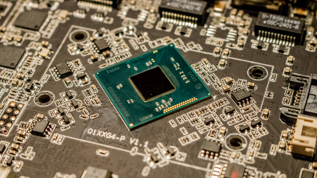
Packaging transforms individual dies into functional chips. Engineers encapsulate each die within a protective casing to shield it from environmental factors like moisture, dust, and physical damage. This process involves attaching the die to a substrate, which serves as a mechanical support and electrical interface. The substrate connects the die to external circuits, enabling seamless integration into electronic devices.
Modern packaging techniques have evolved significantly. Wafer-level packaging, introduced in the early 2000s, allowed manufacturers to package dies directly on the wafer before dicing. This innovation reduced production costs and improved efficiency. Recent advancements, such as 2.5D and 3D stacking technologies, have further enhanced chip performance. These methods utilize through-silicon vias (TSVs) to connect multiple dies vertically, creating compact and powerful chips. These advancements highlight the critical role of packaging in the journey from wafers related to chips to fully functional electronic components.
Adding Connections for Device Integration
After packaging, engineers establish electrical connections between the chip and the device it powers. This step involves creating input and output terminals that link the chip to external circuits. Wire bonding and flip-chip bonding are two common methods used for this purpose. Wire bonding uses fine wires to connect the chip’s terminals to the substrate, while flip-chip bonding directly attaches the chip to the substrate using solder bumps.
The choice of bonding method depends on the chip’s design and application. Flip-chip bonding, for instance, offers higher performance and better heat dissipation, making it suitable for high-performance devices. These connections ensure that the chip communicates effectively with other components, enabling the device to function as intended. Precision during this stage is crucial, as any errors can compromise the chip’s performance and reliability.
Testing and Ensuring Chip Quality
Testing ensures that each chip meets the required standards before it reaches the market. Engineers subject the chips to rigorous tests to verify their functionality, performance, and durability. These tests include electrical testing, thermal testing, and stress testing. Electrical testing checks the chip’s circuits for defects, while thermal testing evaluates its ability to dissipate heat. Stress testing simulates real-world conditions to assess the chip’s reliability over time.
Advancements in testing technologies have improved the accuracy and efficiency of this process. Automated testing equipment (ATE) enables manufacturers to test multiple chips simultaneously, reducing production time. These advancements address challenges such as contamination, precision, and cleanliness, ensuring that only high-quality chips proceed to the next stage. By prioritizing quality assurance, manufacturers uphold the reliability of wafers related to chips, maintaining their critical role in modern electronics.
Why the Relationship Between Wafers, Chips, and Dies Matters
The Role of Chips in Modern Electronics
Chips drive the functionality of modern electronic devices. They serve as the core components in products such as smartphones, laptops, medical equipment, and automotive systems. Each chip, derived from a die, performs specific tasks by processing data, executing instructions, or managing power distribution. Their compact size and efficiency enable manufacturers to create smaller, faster, and more powerful devices.
The versatility of chips extends across various industries. In healthcare, chips power diagnostic tools and wearable devices that monitor vital signs. In telecommunications, they facilitate high-speed internet and seamless communication. Automotive systems rely on chips for advanced driver-assistance systems (ADAS) and electric vehicle (EV) technologies. This widespread application underscores the critical role of wafers related to chips in shaping the technological landscape.
Economic and Technological Impacts of Semiconductor Manufacturing
Semiconductor manufacturing significantly influences global economies and technological progress. The industry creates high-paying jobs, fosters innovation, and drives economic growth. In the United States, initiatives like the CHIPS Act aim to boost domestic production and reduce reliance on foreign suppliers. This investment strengthens the economy while promoting advancements in industries such as automotive, healthcare, and consumer electronics.
East Asia currently dominates semiconductor manufacturing, producing 75% of the world’s supply. However, increased investment in other regions, including the US, is reshaping the global landscape. This shift enhances competition, spurs innovation, and ensures a stable supply chain. The economic benefits extend beyond job creation, as semiconductors enable breakthroughs in artificial intelligence, renewable energy, and quantum computing. These advancements highlight the profound impact of wafers related to chips on both economic and technological fronts.
Innovations in Wafer and Chip Technology
Continuous innovation in wafer and chip technology drives the evolution of modern electronics. Manufacturers are developing smaller, more efficient chips to meet the growing demand for compact and powerful devices. Techniques like wafer-level packaging and 3D stacking enhance chip performance by integrating multiple dies into a single package. These advancements improve energy efficiency, reduce production costs, and enable new applications.
Emerging materials and processes are also transforming the industry. Gallium nitride (GaN) and silicon carbide (SiC) are gaining traction for their superior performance in high-power and high-frequency applications. These materials offer better thermal conductivity and energy efficiency compared to traditional silicon. Additionally, advancements in photolithography, such as extreme ultraviolet (EUV) lithography, allow for the creation of smaller and more intricate circuits. These innovations ensure that wafers related to chips remain at the forefront of technological progress.
Wafers serve as the cornerstone of semiconductor manufacturing, enabling the creation of dies and chips that power modern technology. These thin silicon discs act as the substrate for integrated circuits, forming the basis for countless electronic devices. The transformation from wafers to chips involves precise engineering and advanced processes, highlighting the complexity of semiconductor production. Understanding this relationship reveals the critical role of wafers related to chips in shaping the technological advancements that define daily life. Their significance underscores the intricate craftsmanship behind the devices we rely on every day.
FAQ
What is wafer dicing and its impact on electronic devices?
Wafer dicing refers to the process of cutting a semiconductor wafers into individual dies or chips.
What is the relationship between chips, wafers, and dies in a computer?
Chips, wafers, and dies form an interconnected hierarchy in semiconductor manufacturing. A wafer contains multiple dies, each representing a small section of the wafer etched with circuitry. Each die is then packaged into a chip, which serves as the functional unit in electronic devices. Essentially, a wafer produces many dies, and each die becomes a chip after packaging.
How are semiconductor wafers manufactured?
The manufacturing of semiconductor wafers involves three primary steps:
- Silicon Purification and Refining: Silicon, found in rocks and gravel as silicates or silica, undergoes purification to achieve the required quality.
- Single-Crystal Silicon Growth: Techniques like the Czochralski method grow a single crystal of silicon, ensuring uniformity and purity.
- Wafer Formation: The silicon crystal is sliced into thin wafers, which are then polished to create a smooth surface for circuit fabrication.
These steps ensure that wafers meet the stringent requirements of semiconductor production.
What are the important characteristics of wafers for processing?
Four key characteristics define wafers for processing:
- Wafer Size: Determines the number of dies that can be fabricated on a single wafer.
- Wafer Thickness: Impacts the structural integrity during handling and processing.
- Die Size: Influences the number of chips produced from a wafer.
- Saw Street Width: Refers to the spacing between dies, ensuring precise dicing with minimal material loss.
These attributes play a critical role in optimizing manufacturing efficiency and product quality.
What role do silicon wafers play in integrated circuits?
Silicon wafers act as the foundation for integrated circuits, serving as the substrate on which intricate electronic patterns are etched. Fabrication methods like the Czochralski pulling process and the Float Zone technique ensure high purity and minimal defects. These wafers enable the creation of reliable and efficient electronic components, making them indispensable in modern technology.
What is the Die Preparation process in semiconductor device assembly?
The Die Preparation process involves several steps to prepare individual dies for packaging:
- Wafer Thinning (Backgrinding): Reduces the wafer’s thickness to the desired level.
- Wafer Singulation: Separates the wafer into individual dies through precise dicing.
- Pick and Place: Transfers the separated dies to the next stage of assembly.
Each step includes metrology processes to ensure quality and yield, highlighting the meticulous nature of semiconductor manufacturing.
Why is precision important in wafer dicing?
Precision in wafer dicing ensures that the delicate circuits on each die remain intact. Any deviation during this process can damage the dies, leading to functional defects. Advanced equipment and techniques maintain accuracy, ensuring that each die meets the required specifications. This precision directly impacts the performance and reliability of the final chips.
How do chips power modern electronic devices?
Chips, derived from individual dies, serve as the core components in electronic devices. They process data, execute instructions, and manage power distribution. Their compact size and efficiency enable the development of smaller, faster, and more powerful devices, such as smartphones, laptops, and medical equipment. Chips play a pivotal role in advancing technology across various industries.
What innovations are shaping wafer and chip technology?
Recent innovations in wafer and chip technology include:
- Wafer-Level Packaging: Allows dies to be packaged directly on the wafer, reducing costs and improving efficiency.
- 3D Stacking: Integrates multiple dies vertically using through-silicon vias (TSVs), enhancing chip performance.
- Emerging Materials: Gallium nitride (GaN) and silicon carbide (SiC) offer superior thermal conductivity and energy efficiency for specialized applications.
- Extreme Ultraviolet (EUV) Lithography: Enables the creation of smaller and more intricate circuits.
These advancements drive the evolution of modern electronics, ensuring continuous improvement in performance and functionality.
How does the semiconductor industry impact the global economy?
The semiconductor industry significantly influences global economies by creating high-paying jobs, fostering innovation, and driving technological progress. Initiatives like the CHIPS Act in the United States aim to boost domestic production, reducing reliance on foreign suppliers. This investment strengthens economic stability while promoting advancements in fields such as artificial intelligence, renewable energy, and quantum computing.